What is Atomic Layer Deposition?

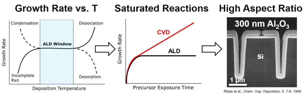
In a typical ALD process, two vapor-phase reagents are sequentially exposed to a heated substrate under low pressure, separated by inert gas purge steps. The combination of these two half cycles constitutes one ALD cycle, which can be repeated in the same cyclic manner to give films with Angstrom-level thickness control. The self-limiting nature, via the making and breaking of chemical bonds, of these half reactions is what gives the ALD process the distinctive features of conformal and uniform films. The uniform and conformal nature of this deposition process is also extended to substrates with complex geometries and high aspect ratios.
Since being first introduced in the 1970s, Atomic layer deposition (ALD) has seen broad adaptation for a variety of uses in the semiconductor industry. ALD has been described as the so-called sister method to chemical vapor deposition, but with some important distinctions. ALD is a vapor phase method to deposit thin films of solid material utilizing sequential, self-limiting half reactions. The surface chemistry involved in ALD ranges from ligand exchange, combustion, and oxidation-reduction, among others. The key advantages of ALD are angstrom-level control over thickness, smooth and conformal coverage in high aspect ratio structures, free of pin-holes, and scalable to large volume manufacturing.
In the semiconductor industry, the use of ALD to deposit thin films has played a pivotal role in the continued device scaling since the 45 nm node (2007), when Intel first adapted using ALD to deposit high-k metal gates. In the years the followed, ALD has made its mark in the industry and has been widely adapted in both front-end-of-line (FEOL) and back-end-of-line (BEOL) processing. Continued progress toward gate-all-around (GAA) and other 3D device architectures (3D NAND and 3D DRAM) only furthers the increased use of ALD in the industry. For example, area-selective ALD has been proposed as an alternative to traditional lithographic patterning techniques. In using ALD to pattern the desired material, continued device scaling can be achieved with a reduction in line-edge roughness, pattern misalignment, and non-uniformity in high aspect ratio structures.
Beyond the semiconductor industry, ALD has seen rapid expansion in the areas such as OLED/optical, solar cells, electrochemical storage, textiles, corrosion resistance, moisture barrier layers, and catalysis, among others. With a broad application base of atomic layer deposition, continued research is required to match the rapid
rise in technological demand.